Samsung on Tuesday outlined when it’s going to launch its 2-nanometer (nm) course of for what purposes within the coming years.
The South Korean tech big mentioned it’s going to start mass manufacturing of 2nm chips to be used in cell purposes in 2025, throughout its Samsung Foundry Discussion board held in San Jose, California.
This implies will probably be providing to make utility processors utilized in smartphones and tablets within the 2nm course of for patrons aiming to launch processors in that dimension.
The nm measurement refers back to the channel size of the transistors that comprise a chip. Superior processors have billions of transistors and their channel size being smaller means extra transistors might be packed in a single chip, making them carry out higher.
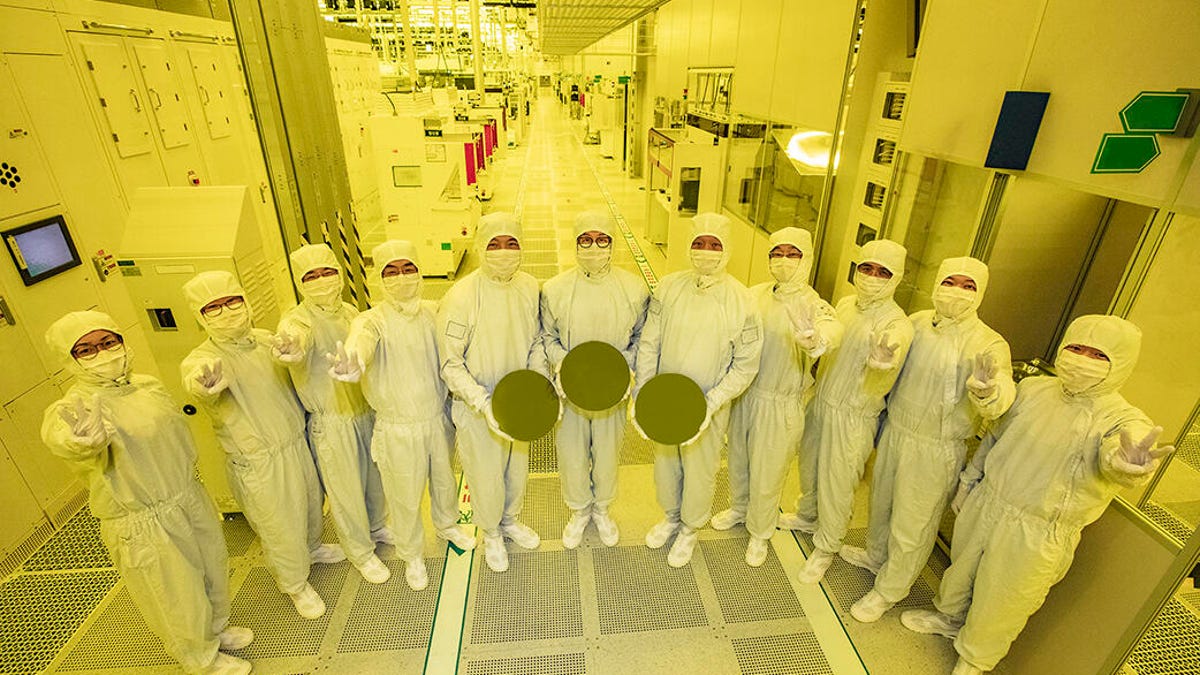
Samsung Foundry, the tech big’s contract chip-producing enterprise unit, affords its manufacturing companies to prospects comparable to Qualcomm and Samsung’s smartphones enterprise unit.
After 2025, Samsung mentioned it’s going to supply 2nm chip manufacturing for high-performance computing in 2026 and in 2027 supply the method for automotive chips.
The corporate mentioned its 2nm course of has proven a 12% enhance and a 25% enhance in efficiency and energy effectivity, respectively, in comparison with its 3nm course of, which it launched final 12 months, the primary amongst chip makers. Samsung mentioned its 2nm course of additionally provided chips 5% smaller in comparison with its 3nm course of.
In the meantime, the corporate reiterated that it’ll start mass manufacturing of chips utilizing its 1.4nm course of in 2027.
In 2025, it’s going to additionally start providing contract manufacturing for 8-inch gallium nitride (GaN) energy administration chips in addition to 5nm RF chips. It would additionally start to supply 8nm and 14nm RF chips for automotive purposes.
Moreover, Samsung is aiming to broaden its clear room capability by 7.3 occasions by 2027 in comparison with 2021. This will likely be achieved via the growth of its fab in Pyeongtaek __ its most superior facility so far __ and its new fab being inbuilt Taylor, Texas, the corporate mentioned. Extra clear rooms imply it’s going to have more room to execute extra orders from prospects.
On the discussion board, Samsung additionally introduced the formation of its Multi-Die Integration Alliance, an alliance with its companions to use new chip packaging applied sciences.
Samsung is the world’s second-largest contract chip producer after TSMC, which manufactures Apple’s A sequence of chips utilized in iPhones.